Analog and Mixed-Signal Design
Savarti analog design team has capability to undertake the most challenging analog design including:
- New design from specification to GDS2
- Porting the designs to advance process nodes to improve design performance
- Design characterization, margin check for first silicon success
- Develop the design modelling such as timing, behavior model or AMS-Verilog model
Savarti design team has experience in development of analog mixed signal verification environment with advanced techniques like UVM. We have designed from Registered-Level, set-up from scratch verification environments, VIP coding, and Test development to final coverage report.
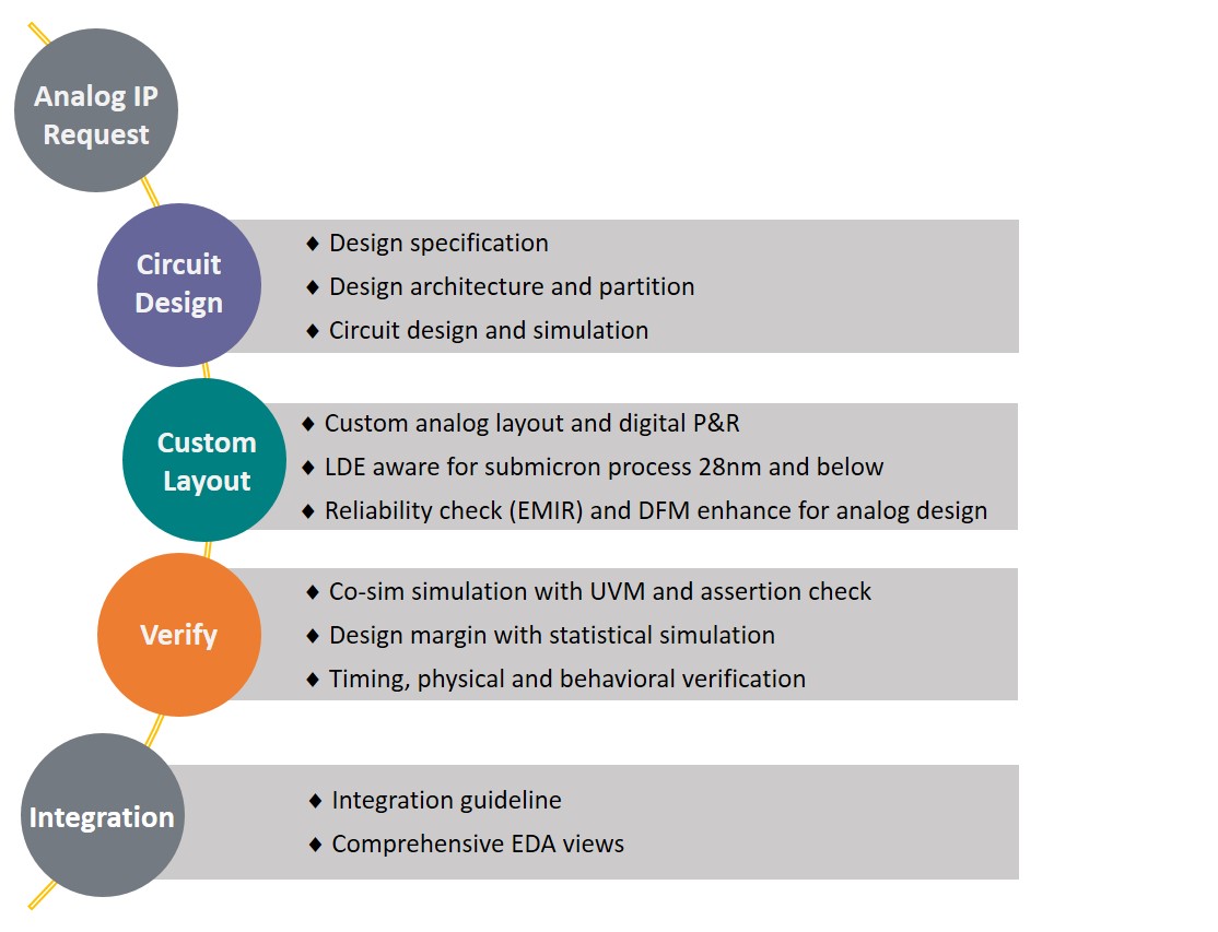
o Integration Guidelines
o ASIC/DFT manufacturing guidelines
o Test and Characterization user guide
o Comprehensive EDA views:
Verilog models
CDL netlists *(.cdl)
ATPG models
GDSII layout
DRC, ERC & LVS reports
Analog & Mixed-Signal IP design services, one of Savarti’s strengths in Integrated Circuit designs. We are a team of highly experienced analog design engineers who are ready to meet any challenges in high-speed design for consumer and networking as well as ultra low-power design for IoT applications.
Savarti has a capability to create high quality analog circuit from scratch and bring them to mass production successfully. And we have proven track records on IP customization and designs from 0.18um to 14nm.
- DDR PHY
- DDR3/4 Combo IO
- Low-power ADPLL
- DDR3/4 PHY macro
- HMB2e PHY
- IO library
- 1.8v to 3.3v GPIO
- I2C and SPI IO
- LVDS and sLVDS IO
- HDMI CEC
- eMMC IO
- Power managements
- On-chip LDO
- Bandgap and reference voltage generator
- Charge pump and voltage rectifier
- Step down DCDC
- Ultra-low power
- Ultra low voltage level shifter 0.4V to 1.2V
- Nano current and voltage reference
- Sub-threshold standard cell library